The advent of nanotechnologies has boosted major developments in electronics and information society, leading to faster, smaller, energy-efficient and more portable systems able to manage and store increasingly higher amounts of information. Key elements in the working principles of nanoelectronic devices are the role played by inter-atomic interactions and quantum mechanical properties such as tunneling and atomistic disorder.
The mission of this IOM research line is to develop and investigate novel nanoscale electronic devices and systems for application in future generations of electronics and information technology, based on alternative, disruptive concepts and architectures.
In this framework, we are active in the synthesis of low-dimensional semiconductor systems for nanoelectronics by Molecular Beam Epitaxy. These include high mobility 2D electron gases for quantum transport applications, hybrid 2D semiconductor-superconductor platforms for scalable quantum computation, as well as semiconductor nanowires for applications in nanoscale electronic devices.

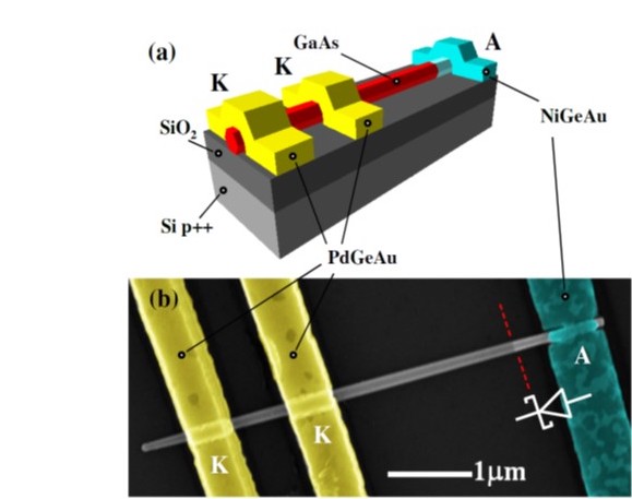
a) Schematic and b) SEM image of a single GaAs nanowire Schottky diode deposited on a Si-SiO2 substrate acting as a back gate. (https://doi.org/10.1103/PhysRevApplied.4.044010)
Another important challenge is to connect the local atomic structure to macroscopic properties of materials and nanostructures
In order to understand and control the physical mechanisms at the base of next-generation electronic devices, our approaches include both experimental analysis -- also by employing large-scale facilities -- and atomistic and multiscale modeling techniques, with applications ranging from non-volatile memories to field-effect and single-molecule electronic devices.

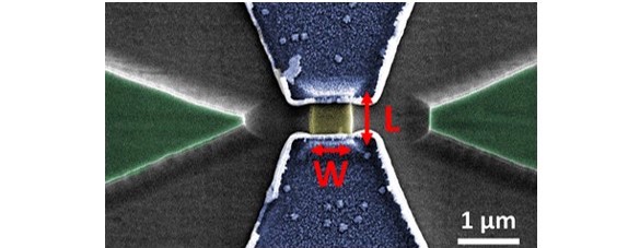
Hybrid superconductor/semiconductor devices (in collaboration with CNR-NANO). Phys. Stat. Sol. RLL 13, 1800222 (2019).